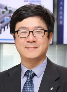
최성율 교수 사진

KAIST전기및전자공학부

양자소자연구실

최성율 교수 (손창근석좌교수, 반도체공학대학원장) (Sung-Yool Choi)

연구실 소개

이 연구실은 MoS₂, MoSe₂ 등 TMDC를 비롯한 2D 반도체 소재의 합성과 단층 박리 방법을 연구합니다. 그래핀과 2D 소재를 차세대 소자 및 대면적 디스플레이에 적용하기 위해 소재의 공정·집적과 유전체, 기판, 채널 및 소스·드레인 사이의 계면을 설계하는 연구를 합니다.

AI가 연구실 홈페이지를 바탕으로 생성한 연구실 소개예요

연구실 홈페이지의 소개

Recently, new semiconducting 2D materials known as transition metal dichalcogenides (TMDCs) appeared, as represented by MoS2, MoSe2, WS2 and WSe2. Unlike graphene field-effect transistors (FETs) with less than ~10 of on/off ratio, the transistors made of these TMDCs can attain high current on/off ratio, which fulfills the current need for the commercial transistors, and the high mobility of TMDCs make the low power consumption of possible. In 2014, we have demonstrated the synthesis of large area MoSe2 via chemical vapor deposition on arbitrary substrates such as SiO2 and Sapphire for the first time. In addition, we have also developed a facile liquid-phase exfoliation method to improve the exfoliation efficiency for single-layer MoS2 or MoSe2 sheets. We are so confident that graphene and 2D materials will play a key role in the development of next-generation nanoscale devices or large-area displays. For the mass production of large-area graphene, CVD is the most popular method. However, handling the CVD-grown 2D materials is difficult due to their extremely thin nature when they are going through the industrial process. Another important subject of the investigation has been the interface engineering between 2D materials and other parts of devices, like the dielectrics, substrates, and channel or source/drain doping process. Integration of high-quality gate dielectrics on graphene is an important technical challenge because the quality of the interface between the dielectrics and graphene channel affects the electrical characteristics of graphene devices, such as operating voltage, scaling capability, and device reliability. To address these issues, we proposed a new approach for integration of high-k dielectrics on graphene using a functionalized graphene monolayer as

원문 보기
연구 분야

Integrated Circuits & Semiconductor Systems · Quantum Science & Engineering · Semiconductor Devices & Nanotechnology · Display Sciences & Engineering · Photonics · 그래핀 · 2D 소자 · 뉴로모픽 소자 · 플렉서블 일렉트로닉스 (Graphene · 2D Devices · Neuromorphic Devices · Flexible Electronics)

졸업생 진로

기업 38명

삼성전자 19 · SK하이닉스 13 · 티맥스소프트 3 · LG디스플레이 2 · 현대자동차 1

학계 10명

광운대학교 1 · 단국대학교 1 · 수원대학교 1 · 인하대학교 1 · 중앙대학교 1 · 한성대학교 1 · KAIST 1 · Kyungpook National University 1 외 2곳

연구기관 2명

ETRI 1 · KIMM 1

연구실 홈페이지에 진로가 적힌 졸업생 50명을 AI가 집계했어요. 적히지 않은 졸업생은 빠져 있고, 지금 소속과 다를 수 있어요. 원문 보기

컨택 준비
[email protected]

홈페이지에서 읽은 구성원

  • 졸업생 1명
컨택 메일 쓰는 법

정보가 틀렸거나 삭제를 원하시면 [email protected]로 알려 주세요.

비슷한 연구를 하는 연구실