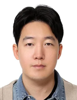
권지민 교수 사진

KAIST전기및전자공학부신생 랩

Device-to-System Integration Laboratory

권지민 조교수 (Jimin Kwon)

홈페이지의 모집 안내

“We are looking for highly motivated students”

원문에서 확인하기
연구실 소개

이 연구실은 실리콘 FET의 미세화 한계에 대응하기 위해 2차원 반도체를 차세대 트랜지스터의 채널 소재로 활용하는 연구를 합니다. 2차원 단일 플레이크의 두께와 균일성이 전기적 특성에 미치는 영향을 분석하고, 전사한 2차원 박막 기반 트랜지스터의 성능과 신뢰성을 연구합니다.

AI가 연구실 홈페이지를 바탕으로 생성한 연구실 소개예요

연구실 홈페이지의 소개

As silicon field-effect transistors approach their fundamental downscaling limits, maintaining performance gains through conventional scaling has become increasingly challenging. To address these limitations, advanced device architectures—such as gate-all-around (GAA) FETs, complementary FETs (CFETs), and FlipFETs—along with emerging low-dimensional channel materials, are being actively explored for next-generation logic. Low-dimensional materials, including two-dimensional transition metal dichalcogenides (TMDs) and one-dimensional carbon nanotubes (CNTs), are particularly attractive due to their excellent electrical properties at scaled dimensions and their compatibility with low-temperature, BEOL-compatible processes. These characteristics make them promising candidates for monolithic 3D integration. enabling sequential device stacking and vertical integration. This work aims to establish a comprehensive framework for employing two-dimensional (2D) semiconductors as channel materials in transistor devices. We first investigate 2D single-flake transistors, focusing on how flake thickness and material uniformity influence electrical characteristics through systematic and statistical analyses. Building on the insights obtained from single-flake devices, we further extend our study to device fabrication using transferred 2D film-based transistor performance. Through this continuous research flow, we seek to bridge fundamental material understanding and practical device implementation of 2D semiconductor channels. This research aims to enhance performance and reliability to enable the commercialization of two-dimensional (2D) semiconductors as transistor channel materials. Focusing on logic-compatible, top-gated 2D FETs, we address key challenges arising from the ultrathi

원문 보기
연구 분야

AI & Machine Learning · Integrated Circuits & Semiconductor Systems · Quantum Science & Engineering · Semiconductor Devices & Nanotechnology · RF · mmWave Devices & Systems · 3D IC and Advanced Packaging · 1D · 2D Logic Devices and DTCO · Oxide Semiconductor Vertical-Channel Transistors for DRAM · 2.5D and 3D Packaging · RF and Quantum Packaging · Chiplet System Architecture

졸업생 진로

기업 1명

삼성SDI 1

학계 1명

한밭대학교 1

기타 2명

KAIST 2

연구실 홈페이지에 진로가 적힌 졸업생 4명을 AI가 집계했어요. 적히지 않은 졸업생은 빠져 있고, 지금 소속과 다를 수 있어요. 원문 보기

컨택 준비
[email protected]

홈페이지에서 읽은 구성원

  • 구성원 20명
  • 졸업생 10명
컨택 메일 쓰는 법

정보가 틀렸거나 삭제를 원하시면 [email protected]로 알려 주세요.

비슷한 연구를 하는 연구실