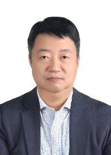
전종욱 교수 사진

성균관대학교전자전기공학부

차세대 반도체 소자 연구실

전종욱 부교수 (Jong Wuk Jun)

연구실 소개

이 연구실은 차세대 반도체 소자 최적화와 집적회로 설계 자동화를 연구합니다. DRAM·NAND Flash·뉴로모픽 메모리, 파운드리 로직, 디스플레이 및 통신 RF 응용을 대상으로 시뮬레이션 기반 AI 자동화와 Digital Twin을 다룹니다. 또한 Path-finding PDK를 활용해 기술 옵션과 기생 효과를 회로 수준에서 예측하고 평가하는 연구를 수행합니다.

AI가 연구실 홈페이지를 바탕으로 생성한 연구실 소개예요

연구실 홈페이지의 소개

성균관대학교 반도체 소자 연구실 (SungKyunKwan University Device Research Laboratory, SKKU-DRL)에서는 전종욱 교수님과 함께 차세대 반도체 소자 최적화 및 집적회로 설계 자동화 기술 연구를 수행하고 있습니다. 특별히, 산업체에서 향후 도입 예정인 메모리(DRAM, NAND Flash, 뉴로모픽) / 파운드리 Logic / 디스플레이 / 통신 RF 응용에 대해, 산업체 기술 개발 flow에 따른 시뮬레이션기반 AI자동화 및 Digital Twin 연구를 수행중에 있습니다. 연구실 목표는 산업계 수요 기반 실무적 기술에 관한 연구 수행을 통해 차세대 반도체 기술 개발을 주도적으로 수행할 수 있는 고급 엔지니어 양성에 있습니다. PDK is a database that specifies a technology; it contains all the information required to design an IC. “Path-finding PDK“ incorporates data about future technology (device electrical properties, mask info., design rules, types and layout of cells, etc.) where options have not been decided or standardized, path-finding PDK includes various options. The designers can then make their early design studies trying out the available options. In addition, in the latest technologies, the parasitic effects such as parasitic RC delay, IR drop, local strain effect, and self-heating etc. becomes very important and they are strongly dependent on the design layout style. So, the accurate estimation of various technology options can be performed at the circuit level. That’s why we need path-finding PDK. Device engineers and designers have started to discuss exploiting the concept of virtual fabrication in order to hedge the risk arising from difficulties in optimizing many new knobs simultaneously. Concurrent optimization of design and technology based on prediction of semiconductor hardware characteristics has now become an integral component of technology development. Traditional design and technology co-optimization (DTCO) has focused on the interplay between technology (device architecture and integration) and design (design rule and layout scheme) in terms of design for manufacturability. As silicon scaling

원문 보기
연구 분야

Semiconductor CAD (Device Simulation, Circuit Modeling and Design automation)

졸업생 진로

기업 23명

삼성전자 6 · Micron Technology 4 · SK하이닉스 3 · 알세미 2 · 대한항공 1 · 동진쎄미켐 1 · 세미브레인 1 · IMS Nanofabrication 1 외 4곳

연구기관 1명

한국나노기술원 1

기타 1명

반도체산업협회 1

연구실 홈페이지에 진로가 적힌 졸업생 25명을 AI가 집계했어요. 적히지 않은 졸업생은 빠져 있고, 지금 소속과 다를 수 있어요. 원문 보기

컨택 준비
[email protected]

홈페이지에서 읽은 구성원

  • 박사과정 25명
  • 구성원 2명
  • 졸업생 22명
컨택 메일 쓰는 법

정보가 틀렸거나 삭제를 원하시면 [email protected]로 알려 주세요.

비슷한 연구를 하는 연구실