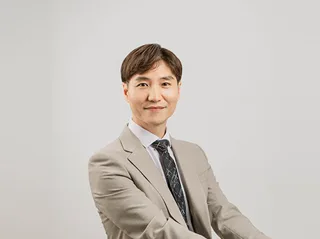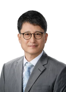
박희천 교수 사진

UNIST전기전자공학과신생 랩

반도체설계자동화연구실

박희천 조교수 (Heechun Park)

연구실 소개

이 연구실은 3D IC와 2.5D 칩렛 시스템 등 첨단 적층형 집적회로 아키텍처를 위한 EDA 방법론을 연구합니다. 첨단 공정 노드에서의 신뢰성 있는 물리 설계와 설계·공정·기술 간 최적화, 딥러닝·강화학습·GPU 가속·생성형 AI를 활용한 EDA 알고리즘을 다룹니다. 또한 LiM, PIM, CiM 등 인메모리 컴퓨팅 기반 AI 칩의 물리 설계 최적화를 연구합니다.

AI가 연구실 홈페이지를 바탕으로 생성한 연구실 소개예요

연구실 홈페이지의 소개

We develop EDA methodologies for advanced stacked IC architectures, including 3D ICs with memory-on-logic and logic-on-logic integration, backside and dual-side interconnect technologies, and 2.5D chiplet systems based on interposers. We develop DRV-aware design methodologies for advanced technology nodes, focusing on robust physical design and cross-layer optimization through design-technology co-optimization (DTCO) and system-design-technology co-optimization (SDTCO). Our AI-EDA research develops intelligent algorithms for next-generation electronic design automation, spanning deep-learning-based design quality prediction, reinforcement-learning-driven design optimization, GPU-accelerated differentiable optimization, and generative AI for automated circuit and system design. We develop EDA/CAD methodologies for emerging AI chip architectures, focusing on physical design optimization for in-memory computing systems, including logic-in-memory (LiM), processing-in-memory (PIM), and compute-in-memory (CiM).

원문 보기
연구 분야

인공지능 및 컴퓨터 · 집적회로 설계 · computer-aided design (CAD) solutions for SoC & VLSI · build electronic design automation (EDA) frameworks

컨택 준비
[email protected]

홈페이지에서 읽은 구성원

  • 박사과정 16명
  • 학부 인턴 23명
컨택 메일 쓰는 법

정보가 틀렸거나 삭제를 원하시면 [email protected]로 알려 주세요.

비슷한 연구를 하는 연구실