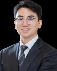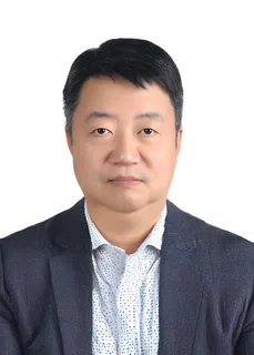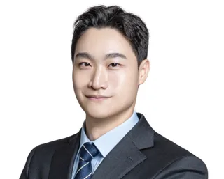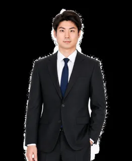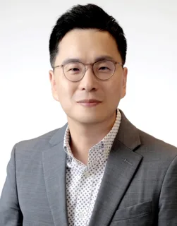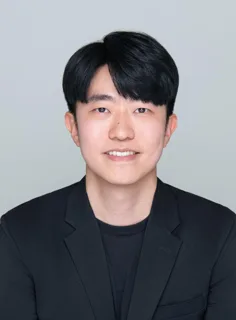
김형진 교수 사진

한양대학교신소재공학부

반도체소자 연구실(Semiconductor Devices Lab)

김형진 부교수 (Hyungjin Kim)

홈페이지의 모집 안내

“We are looking for highly-motivated undergraduate students (3~4학년), and graduate students who are interested in semiconductor materials, devices, and fabrication. Please feel free to contact Prof. Hyungjin Kim (hkim12 at hanyang.ac.kr). [”

원문에서 확인하기
연구실 소개

이 연구실은 차세대 반도체 소자와 어레이 구조의 전기적 특성을 TCAD 시뮬레이션으로 예측하고, 소자를 제작해 성능을 측정·분석합니다. Si 플래시와 멤리스터 등의 메모리 어레이를 기반으로 신경모사 시스템, 하드웨어 보안, 논리 연산 등 컴퓨팅 응용을 연구합니다.

AI가 연구실 홈페이지를 바탕으로 생성한 연구실 소개예요

연구실 홈페이지의 소개

본 연구실은 차세대 반도체 소자 및 어레이 구조에서의 컴퓨팅 응용 연구를 수행하고 있습니다. TCAD 툴 시뮬레이션을 통해 반도체 소자의 전기적 특성을 예측하고, 이를 반도체 공정 과정을 통해 직접 제작하여 성능 측정평가 및 분석을 수행합니다. 또한, Si 플래시, 멤리스터 등의 메모리 반도체 어레이 구조를 기반으로 신경모사 시스템, 하드웨어 보안, 논리 연산 등 다양한 컴퓨팅 응용 분야를 연구하고 있습니다. 이 과정에서 재료, 공정, 소자, 회로, 시스템, 알고리즘 등이 포함된 융복합적인 연구를 수행하고 있습니다. Our research focuses on emerging semiconductor devices and arrays, exploring their computing applications. We predict the electrical characteristics of these devices through TCAD tool simulations, fabricate them, and analyze the measured data. Additionally, we investigate various computing applications, including neuromorphic systems, hardware security, and logic operations based on memory array structures such as Si flash and memristors. Throughout this process, we conduct interdisciplinary research encompassing materials, processes, devices, circuits, systems, and algorithms.

원문 보기
연구 분야

반도체 공정 · 소자 및 컴퓨팅 응용 · Semiconductor Processes · Devices · and Computing Applications

졸업생 진로

기업 5명

ASML 1 · Keysight Technologies 1 · KLA 1 · LG디스플레이 1 · SK하이닉스 1

진학 1명

한양대학교 1

연구실 홈페이지에 진로가 적힌 졸업생 6명을 AI가 집계했어요. 적히지 않은 졸업생은 빠져 있고, 지금 소속과 다를 수 있어요. 원문 보기

컨택 준비
[email protected]

홈페이지에서 읽은 구성원

  • 석박통합과정 7명
  • 학부 인턴 3명
컨택 메일 쓰는 법

정보가 틀렸거나 삭제를 원하시면 [email protected]로 알려 주세요.
비슷한 연구를 하는 연구실