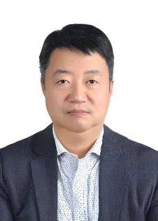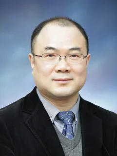
강석형 교수 사진

포항공과대학교전자전기공학과

CAD 및 SoC 설계 연구실

강석형 교수 (Seokhyung Kang)

연구실 소개

이 연구실은 휴리스틱 기법과 인공지능을 결합해 반도체 칩의 전력·성능·면적(PPA)을 개선하는 전자설계자동화(EDA)를 연구합니다. 물리 설계, 아날로그 회로 최적화, 표준 셀 생성, 설계-기술 공동 최적화(DTCO)를 다루며, 물리 설계와 설계 공간 최적화(DSO)의 예측·최적화·생성에 머신러닝과 강화학습을 적용합니다.

AI가 연구실 홈페이지를 바탕으로 생성한 연구실 소개예요

연구실 홈페이지의 소개

The smartphones we use, autonomous vehicles on the road, and even AI servers all run on highly advanced semiconductor chips. These chips contain billions of transistors and intricate circuits, far too complex and time-consuming to design by hand. Electronic Design Automation (EDA) refers to the software tools and technologies that make it possible to design and verify such chips. With EDA, engineers can automatically draw circuits, optimize layouts, and analyze power and performance. This enables the creation of smaller, faster, and more efficient semiconductors, which serve as the foundation for innovations in AI, autonomous driving, healthcare, and many other fields. Recently, artificial intelligence and machine learning have also been applied to EDA, helping analyze massive design data and discover improved methods for chip design that would be difficult for humans to achieve alone. Our lab focuses on Electronic Design Automation (EDA) to improve power, performance, and area (PPA) of semiconductor chips by combining heuristic methods with artificial intelligence. Our research covers the full spectrum of chip design, including physical design, analog circuit optimization, standard cell generation, and design-technology co-optimization (DTCO). We place particular emphasis on applying machine learning (ML) and reinforcement learning (RL) to prediction, optimization, and generation tasks across physical design and design space optimization (DSO).

원문 보기
연구 분야

집적회로 설계 자동화 (VLSI CAD) · 시스템온칩 설계 (SoC design)

졸업생 진로

기업 3명

SK하이닉스 2 · 리벨리온 1

연구실 홈페이지에 진로가 적힌 졸업생 3명을 AI가 집계했어요. 적히지 않은 졸업생은 빠져 있고, 지금 소속과 다를 수 있어요. 원문 보기

정보가 틀렸거나 삭제를 원하시면 [email protected]로 알려 주세요.

비슷한 연구를 하는 연구실