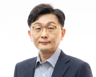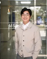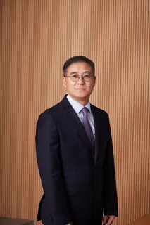
양철웅 교수 사진

성균관대학교신소재공학부

전자현미경 연구실

양철웅 교수 (Cheolwoong Yang)

홈페이지의 모집 안내

“고온·전류 인가 환경에서 SAC305 솔더 접합부의 Cu-Sn 금속간화합물(IMC) 성장 및 미세구조 변화를 연구할 석사과정생을 모집합니다.”

원문에서 확인하기
연구실 소개

이 연구실은 전자현미경을 활용해 상변화 메모리의 원자 배열과 상전이 기작, 셀렉터의 스위칭 기작을 분석합니다. 또한 ReRAM의 저항 변화와 고장 원인을 규명하고, 재료의 미세구조와 특성 간 관계를 실시간 관찰하는 전자현미경 분석 기법을 연구합니다.

AI가 연구실 홈페이지를 바탕으로 생성한 연구실 소개예요

연구실 홈페이지의 소개

The interfacial phase-change memory fabricated using a superlattice, a cross-stack of GeTe and Sb2Te3, can implement a phase transition from high-resistance to low-resistance without going through an amorphous state. This new device exhibits superior characteristics, such as faster phase-change rate, lower reset current, and higher cyclability compared to conventional phase-change memory. However, there are various opinions on the atomic arrangement of the high and low resistance states and the lattice structure model of the superlattice phase change memory, and there are no clearly proven observations. In this study, an in-situ transmission electron microscopy is used to reveal the structure of the superlattice as well as to investigate the phase transition mechanism. In addition, research on selectors to improve noise problems between cells as well as cells themselves is very important. The switching mechanism of the selector is being investigated using in-situ transmission electron microscopy. The ReRAM(resistive switching random access memory) is a memory device that stores information using a phenomenon that causes a change in the resistance through the formation and rupture of a conductive filament(CF) with a width of several nm. ReRAM, with its outstanding performance and similarity to the synaptic connection of neurons, is drawing attention as a new next-generation memory. Our group is testing a new material system for high-performance ReRAM and is analyzing devices using an in-situ TEM technique to elucidate the mechanism of resistance change and failure. In-situ electron microscopy (real-time observation technique) can provide dynamic information for understanding the relationship between the properties of the material and the microstructure by observing the c

원문 보기
연구 분야

전자현미경을 기반으로 한 재료 분석 및 전자현미경 분석 기법의 개발 · 실시간 관찰 투과전자현미경 홀더 개발 및 복합적인 동적환경에서의 실시간 관찰 · 다양한 재료에서의 계면 반응 분석 · 반도체 소자의 미세구조 분석 및 불량원인 분석 · 저차원 물질의 합성 및 분석

졸업생 진로

기업 30명

삼성전자 13 · 삼성전기 2 · LG Philips 2 · SK하이닉스 2 · 두산 1 · 창성 1 · 현대제철 1 · 온세미컨덕터 1 외 7곳

학계 1명

전남대학교 1

연구기관 8명

한국과학기술연구원 2 · Ames National Laboratory 2 · 한국세라믹기술원 1 · 한국자동차연구원 1 · 한국에너지기술연구원 1 · 한국기초과학지원연구원 1

기타 3명

성균관대학교 2 · 원국제특허법률사무소 1

연구실 홈페이지에 진로가 적힌 졸업생 42명을 AI가 집계했어요. 적히지 않은 졸업생은 빠져 있고, 지금 소속과 다를 수 있어요. 원문 보기

컨택 준비
[email protected]

홈페이지에서 읽은 구성원

  • 졸업생 45명
컨택 메일 쓰는 법

정보가 틀렸거나 삭제를 원하시면 [email protected]로 알려 주세요.

비슷한 연구를 하는 연구실