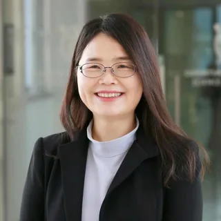
김미영 교수 사진

서울대학교재료공학부

Electron Microscopy & Spectroscopy Lab

김미영 Professor (Miyoung Kim)

연구실 소개

이 연구실은 첨단 소재의 구조와 물성 간 관계를 이해하기 위해 원자 분해능 STEM/EELS, CBED, 전자 홀로그래피, TEM 내 전기 바이어스 실험 등을 활용합니다. DFT 계산을 통해 소재의 원자·전자 구조와 물성을 연관 지으며, 새로운 기능성 소재와 소자 설계를 연구합니다.

AI가 연구실 홈페이지를 바탕으로 생성한 연구실 소개예요

연구실 홈페이지의 소개

The primary goal of our research is to understand the structure-property relationship in advanced materials, for which we utilize several advanced TEM-related techniques including atomic-resolution STEM/EELS, CBED, electron holography or in-situ electrical biasing experiment. Furthermore, we try to correlate atomic and electronic structures of advanced materials with their physical properties using DFT calculations. Our group members are trained to be experts in the characterization of advanced materials. We believe that our research further leads to designing functional materials or devices of new concept.

원문 보기
연구 분야

Crystal structures · Electronic structures · Nano scale measurements of charge distribution and strain fields · In-situ I-V measurements in TEM · Electronic Materials

졸업생 진로

기업 7명

삼성전자 4 · SK하이닉스 2 · 에스케이온 1

학계 3명

금오공과대학교 1 · Harvard University 1 · University of Illinois Chicago 1

연구기관 2명

Diamond Light Source 1 · Oak Ridge National Laboratory 1

진학 2명

Northeastern University 1 · University of Illinois Urbana-Champaign 1

연구실 홈페이지에 진로가 적힌 졸업생 14명을 AI가 집계했어요. 적히지 않은 졸업생은 빠져 있고, 지금 소속과 다를 수 있어요. 원문 보기

컨택 준비
[email protected]

홈페이지에서 읽은 구성원

  • 박사과정 13명
  • 구성원 2명
  • 졸업생 14명
컨택 메일 쓰는 법

정보가 틀렸거나 삭제를 원하시면 [email protected]로 알려 주세요.

비슷한 연구를 하는 연구실