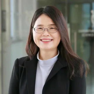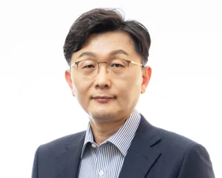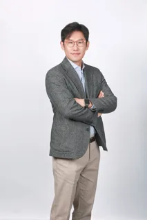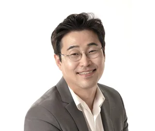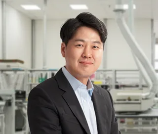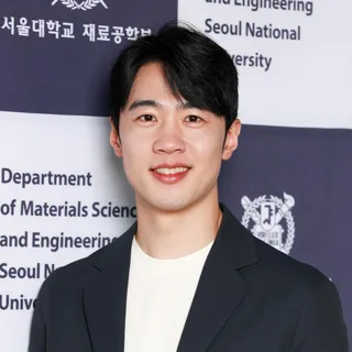
유효빈 교수 사진

서울대학교재료공학부

Hyobin Yoo research group at SNU (서울대학교 재료공학부 유효빈 교수 연구실)

유효빈 Associate Professor (Hyobin Yoo)

홈페이지의 모집 안내

“We are currently looking for new members to our group. Exciting research opportunities for graduate/undergraduate students and post-doc candidates are now open!”

원문에서 확인하기
연구실 소개

이 연구실은 operando TEM과 정밀 전기 측정을 활용해 재료와 소자의 원자 수준 구조, 물성 및 기능을 이해하고 제어하는 연구를 합니다. 2차원 van der Waals 결정으로 계면과 moiré 초격자를 만들고 원자 구조를 조절해 양자 전자 현상을 살피며, TEM과 STEM으로 재료의 구조를 원자 수준까지 분석합니다.

AI가 연구실 홈페이지를 바탕으로 생성한 연구실 소개예요

연구실 홈페이지의 소개

The primary objective of our research group is to advance atomic-scale engineering capabilities in both materials and devices. We achieve this by exploiting operando transmission electron microscopy (TEM), integrating state-of-the-art atomic resolution TEM techniques with modern semiconductor device fabrication and precise electrical measurements. Our research emphasizes a comprehensive understanding and control of material properties and device functionalities at the atomic scale. By leveraging atomic-scale structural and chemical characterization along with precision fabrication techniques, we aim to develop novel materials and devices with unprecedented performance. This research drives innovation at the intersection of materials science and device engineering, leading to technological breakthroughs and a deeper understanding of material behavior at its most fundamental level. We engineer novel designer interface by assembling various 2-D van der Waals building block crystals. By creating moiré superlattice and engineering the atomic scale reconstruction, we seek to investigate the emergent phenomena that exhibit quantum electronic behavior. Our group employs transmission electron microscopy (TEM) and scanning transmission electron microscopy (STEM) to investigate the structures of materials from microscale down to the very atomic scale. Understanding the electron optics inside the microscopy and electron diffraction in crystals is key to investigate the structures of condensed matter. We study the atomic structure to understand the underlying materials properties and functionalities. Our group develops a new platform that enables the simultaneous operation of electronic devices and transmission electron microscopy (TEM) investigations. By applying modern semiconduct

원문 보기
연구 분야

Operando transmission electron microscopy · Cryo transmission electron microscopy · Electrical measurements and functional characterization · Electronic Materials

컨택 준비
[email protected]

홈페이지에서 읽은 구성원

  • 구성원 9명
컨택 메일 쓰는 법

정보가 틀렸거나 삭제를 원하시면 [email protected]로 알려 주세요.

비슷한 연구를 하는 연구실