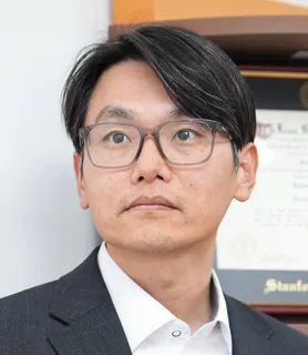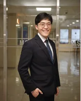
이가영 교수 사진

KAIST전기및전자공학부

Low-dimensional Electron Systems Lab

이가영 부교수 (Kayoung Lee)

홈페이지의 모집 안내

“We are looking for ambitious, diligent, and highly motivated students!”

원문에서 확인하기
연구실 소개

이 연구실은 2차원 소재에서 양자 홀 효과와 위상·양자 스핀 홀 상태 등 양자 현상을 연구하고, 양자 상태의 에너지를 측정하는 기법과 나노소재의 제작·특성 분석 방법을 개발합니다. 또한 2D 반도체의 접촉 저항과 페르미 준위 고정 문제를 개선하는 접촉 구조를 연구하고, 양극성 및 재구성 가능한 소자와 이를 활용한 회로를 개발합니다.

AI가 연구실 홈페이지를 바탕으로 생성한 연구실 소개예요

연구실 홈페이지의 소개

High mobility transistors, steep-slope transistors, low-power tunneling electronics, multi-valued logics, electronic sensors, contact property optimization etc. We are interested in various quantum phenomena such as quantum Hall effect and topological/quantum spin Hall states in two-dimensional materials. In such nanoscale materials due to the reduced dimensionality quantum effect can be pronounced. Using our non-local Fermi energy measurement technique we are capable of direct probing of energy of such quantum states. We design novel condensed matter systems, study new quantum phenomena, and explore practical nanoelectronics using emerging nanoscale materials and physics. This research includes developing new method of nano fabrication and precise characterization techniques. 2D materials show great promise as potential replacements for silicon, primarily because they do not suffer from performance degradation caused by miniaturization. Nevertheless, the broader implementation of 2D semiconductors faces certain challenges, such as high contact resistance and Fermi level pinning issues. These limitations pose obstacles to the practical utilization of 2D semiconductors in various fields, particularly in the development of CMOS circuits and systems because p-type 2D semiconductor options are highly restricted. We have recently achieved realization of ambipolar characteristics of 2D MoS2 and InSe by developing advanced van der Waals contacts that relieve the Fermi-level pinning without forming defects at the surface of semiconductors. This allowed us to invent unprecedented strategies to achieve superior ambipolar characteristics and complementary reconfigurable multifunctionality. We also aim to demonstrate circuits composed of such reconfigurable devices and validate the

원문 보기
연구 분야

Integrated Circuits & Semiconductor Systems · Quantum Science & Engineering · Semiconductor Devices & Nanotechnology · Photonics · Low-dimensional materials · semiconductor physics · nanostructure electron devices

졸업생 진로

기업 5명

삼성전자 5

연구기관 1명

한국세라믹기술원 1

연구실 홈페이지에 진로가 적힌 졸업생 6명을 AI가 집계했어요. 적히지 않은 졸업생은 빠져 있고, 지금 소속과 다를 수 있어요. 원문 보기

컨택 준비
[email protected]

홈페이지에서 읽은 구성원

  • 석박통합과정 1명
  • 학부 인턴 15명
  • 구성원 4명
  • 졸업생 56명
컨택 메일 쓰는 법

정보가 틀렸거나 삭제를 원하시면 [email protected]로 알려 주세요.

비슷한 연구를 하는 연구실