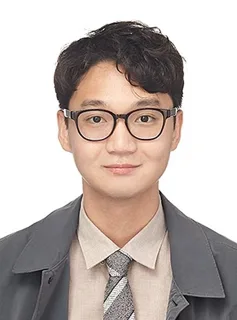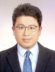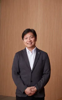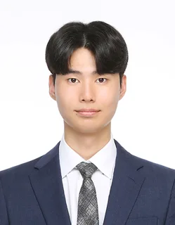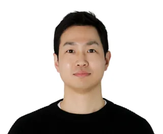
김병조 교수 사진

UNIST신소재공학과신생 랩

가상재료공정설계 연구실

김병조 조교수 (Byungjo Kim)

홈페이지의 모집 안내

“We are recruiting postdoctoral researchers, graduate students, and undergraduate interns in materials, mechanics, and AI. Contact Byungjo Kim for positions at the quantum–continuum interface.”

원문에서 확인하기
연구실 소개

이 연구실은 길이·시간·물리 영역에 걸쳐 나타나는 재료 및 공정 현상을 멀티스케일 모델로 분석하고, 각 규모의 모델을 연결해 예측하는 방법을 연구합니다. 반도체 표면과 계면, 식각·증착, 박막 성장, 반응기 내 수송과 장비 조건을 대상으로 시뮬레이션과 실험 데이터를 결합한 디지털 트윈을 구축하고, AI를 활용해 공정 상태를 예측하고 최적화합니다.

AI가 연구실 홈페이지를 바탕으로 생성한 연구실 소개예요

연구실 홈페이지의 소개

VDLab investigates phenomena that span scales, turns that understanding into virtual models for materials, processes, and equipment, and connects those models to experiments and physical manufacturing through AI. Semiconductor manufacturing is our primary proving ground, while functional materials broaden the design space. Many engineering systems are governed by phenomena that cross length, time, and physical domains. We develop first-principles, atomistic, mesoscale, feature-scale, and continuum models, then connect them with physics-based and data-driven scale bridging. The result is not a collection of isolated simulations but a predictive description that carries mechanisms and uncertainty across scales. We turn computational understanding into design variables and decisions. Our work spans semiconductor surfaces and interfaces, etching and deposition, film growth, reactor transport, and equipment conditions, with AI and optimization used to explore spaces that are too large for trial and error. The same methodology extends to broader functional materials. Advanced Manufacturing AI begins when virtual models and physical systems share information. We combine simulation, experimental databases, in-situ sensing, and reduced-order models in digital twins that can estimate hidden process states, explain predictions, and support optimization and control. Physical AI and agentic systems are the path toward closing this loop from observation to action. Couples virtual process simulation with physical measurement to model and predict ultra-precision cryogenic etching. A virtual–physical AI digital twin for the fabrication processes of advanced semiconductor devices. Industry-commissioned platform for simulation-based analysis and prediction of nanostructure deposition proc

원문 보기
연구 분야

멀티스케일 시뮬레이션 · 반도체 재료 · 재료 공정 · 플라즈마-재료 상호작용 · 머신러닝 기반 재료 설계 · 분자동역학 · 나노복합재 · 전산모델링 · B. Kim · M. Kim* · S. Yoo · S. K. Nam · Applied Surface Science. Elsevier · 2022 · 08

컨택 준비
[email protected]

홈페이지에서 읽은 구성원

  • 학부 인턴 7명
컨택 메일 쓰는 법

정보가 틀렸거나 삭제를 원하시면 [email protected]로 알려 주세요.

비슷한 연구를 하는 연구실