홈페이지의 모집 안내
“We are seeking research fellows, postdoctoral researchers, graduate students, and undergraduate students interested in joining our group.”
원문에서 확인하기정보가 틀렸거나 삭제를 원하시면 [email protected]로 알려 주세요.
홈페이지의 모집 안내
“We are seeking research fellows, postdoctoral researchers, graduate students, and undergraduate students interested in joining our group.”
원문에서 확인하기이 연구실은 3D Bulk FinFET과 3D NAND Flash Memory 등 비휘발성 메모리 소자, 박막 트랜지스터, 유연 전자소자와 가스·바이오 센서를 연구합니다. 또한 뉴로모픽 및 재구성형 소자·회로를 다루며, 소자의 제작·측정·특성 분석·모델링을 수행합니다.
AI가 연구실 홈페이지를 바탕으로 생성한 연구실 소개예요
연구실 홈페이지의 소개
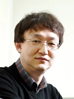
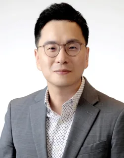
Prof. Lee is a Lifetime Member of the Institute of Electronics Engineers of Korea (IEEK) and IEEE Fellow. He has been served as a subcommittee member of IEDM, ITRS ERD member, a general chair of IPFA2011, and IEEE EDS Korea chapter chair. He received many awards for excellent research papers and research excellence. He invented bulk FinFET, Saddle FinFET (or bCAT) for DRAM cell transistors, and NAND flash cell string with virtual source/drain. These three inventions are key technologies which have been applying for mass production in industry. We are seeking research fellows, postdoctoral researchers, graduate students, and undergraduate students interested in joining our group. Our laboratory is a group of Semiconductor Materials and Devices Laboratory (SMDL) at the department of Electrical and Computer Engineering in Seoul National University. A field of research covers nonvolatile memory, flexible electronics, gas sensors & bio sensors, thin film transistors (TFTs), reconfigurable devices & circuits, and neuromorphic devices & circuits. The devices and circuits are fabricated mainly at ISRC (Inter-University Semiconductor Research Center) located inside the campus of Seoul National University. Most of students in our laboratory have an experience to fabricate semiconductor devices and circuits by themselves. Some of devices and circuits are provided from semiconductor companies through collaboration projects. The scope of research in our laboratory includes device fabrication, measurement, characterization, and modeling. We have five probe stations (probe card, temperature, gas, moisture, laser light), four semiconductor parameter analyzers, oscilloscope, spectrum analyzer, low noise current/voltage amplifier, lock-in amplifier, laser light sources (650 nm, 550 nm, 4
정보가 틀렸거나 삭제를 원하시면 [email protected]로 알려 주세요.
| 연구실 | 대학 | 주요 주제 | 구성원 | 비교 |
|---|---|---|---|---|
나노 전자 및 신경망 모사 소자 연구실조병진 교수 | KAIST | 반도체 소자회로·칩 설계광학·포토닉스 | – | |
나노 전자소자 및 재료 연구실(Nano Electronic Devices & Materials Lab)최창환 교수 | 한양대 | 반도체 소자나노소재 | – | |
전자소자 연구실(EDL)김현재 교수 | 연세대 | 센서·MEMS태양전지반도체 소자 | – | |
반도체 소자 연구실신형철 교수 | 서울대 | 반도체 소자 | 2 | |
지능형 반도체 시스템 연구실송윤흡 교수 | 한양대 | 반도체 소자디스플레이 | – | |
차세대 반도체 및 뉴로모픽 소자 연구실김영훈 교수모집 안내 | 성균관대 | 반도체 소자센서·MEMS | 13 |