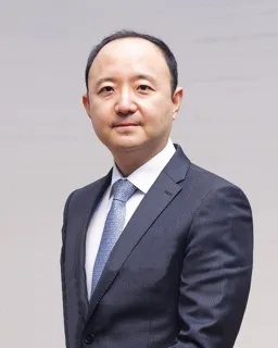
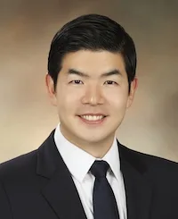
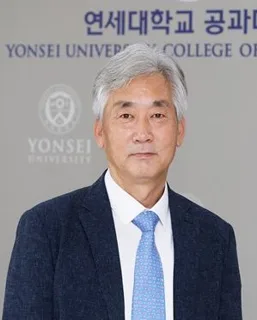
이 연구실은 용액 공정 기반 전자·광전자소자에서 전하·엑시톤·열 수송과 계면이 소자 특성에 미치는 영향을 연구합니다. 퀀텀닷 발광다이오드의 효율과 안정성, 풀컬러 패터닝, 유기반도체 기반 열전·뉴로모픽 소자와 소자물리를 다룹니다.
AI가 연구실 홈페이지를 바탕으로 생성한 연구실 소개예요
연구실 홈페이지의 소개
We investigate how charge, excitons, heat, and interfaces govern solution-processed electronic and optoelectronic devices. By connecting fundamental transport physics with device architecture, scalable processing, and data-driven analysis, we develop light-emitting, energy-harvesting, and adaptive electronic systems. AONE Lab engineers quantum-dot light-emitting diodes (QLEDs) across the full device hierarchy, from charge injection and nanoscale interfaces to optical structures and full-color patterning. We combine steady-state and transient electrical and optical measurements with simulation and machine learning to determine how transport layers, QD films, and device architecture govern efficiency, brightness, and operational stability. Our goal is to translate fundamental device physics into robust display technologies across scales, including microdisplay-oriented, top-emission, large-area, flexible, and transparent platforms. Charge injection, transport, balance, recombination, and exciton–charge dynamics under electrical operation. QD/transport-layer interfaces, ZnO- and ZnMgO-based electron-transport layers, degradation pathways, and operational lifetime. Ultra-high-brightness, top-emission, and optical-cavity structures, together with flexible, stretchable, and transparent devices. Full-color QD patterning through photolithography, electrophoretic deposition, and inkjet printing, including analysis of process-induced changes. OLEDs and other organic optoelectronic devices provide complementary systems for investigating charge transport, interfaces, and mechanically compliant architectures. We investigate electronic and thermal transport in solution-processable semiconductors and engineer thin-film thermoelectric systems that convert low-grade or spatially complex
정보가 틀렸거나 삭제를 원하시면 [email protected]로 알려 주세요.
| 연구실 | 대학 | 주요 주제 | 구성원 | 비교 |
|---|---|---|---|---|
광전자나노소재및소자연구실임재훈 교수모집 안내 | 성균관대 | 반도체 소자나노소재광학·포토닉스 | – | |
양자점 에너지 및 반도체 소자 연구실최민재 교수 | 성균관대 | 반도체 소자센서·MEMS촉매·수소·연료전지 | 6 | |
고분자/유기 반도체 연구실김봉수 교수 | UNIST | 반도체 소자고분자유기화학·합성 | 8 | |
Organic Semicondcutor Optoelectronics Laboratory조환희 교수 | 연세대 | 반도체 소자무기·물리화학 | 9 | |
지능형 디스플레이 및 센서 연구실이재상 교수 | 서울대 | 반도체 소자광학·포토닉스디스플레이 | 8 | |
Information & Electronic Materials Research Lab (IEMR)명재민 교수모집 안내 | 연세대 | 센서·MEMS나노소재광학·포토닉스 | 7 |