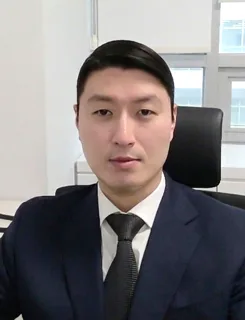
김기석 교수 사진

성균관대학교신소재공학부신생 랩

첨단플라즈마나노공정연구실

김기석 조교수 (Kiseok Kim)

연구실 소개

이 연구실은 복잡한 3차원 구조에서 원자층 식각의 선택성과 정밀도를 높이고, 저온 플라즈마 화학과 프로파일 제어를 활용해 손상을 줄인 고종횡비 구조를 형성하는 공정을 연구합니다. VHF·이중 주파수·펄스 플라즈마 공정을 최적화하고, 단결정 2D·3D 소재를 활용한 로직-온-메모리 집적과 이종 소재 적층을 연구합니다.

AI가 연구실 홈페이지를 바탕으로 생성한 연구실 소개예요

연구실 홈페이지의 소개

Selective Atomic Layer Etching (ALE): Achieving sub-nanometer precision and atomic-scale selectivity for complex 3D architectures. Cryogenic & Directional Etching: Leveraging low-T plasma chemistry and precise profile engineering (anisotropic/isotropic) for damage-free, HAR structures. Advanced Plasma Engineering: Optimization of VHF (30-162 MHz), Dual-frequency, and Pulsed plasma processes for seamless material integration. Expertise in leveraging single-crystalline 2D/3D materials for next-generation semiconductor architectures, focusing on logic-on-memory integration and heterogeneous material stacking to enable advanced multi-functional devices.

원문 보기
연구 분야

초미세 플라즈마 나노 공정 · 선택적 원자층 식각 · 3차원 적층형 반도체 나노 소자

컨택 준비
[email protected]

홈페이지에서 읽은 구성원

  • 석박통합과정 4명
컨택 메일 쓰는 법

정보가 틀렸거나 삭제를 원하시면 [email protected]로 알려 주세요.

비슷한 연구를 하는 연구실