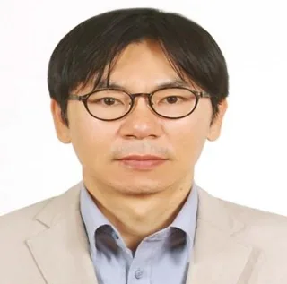
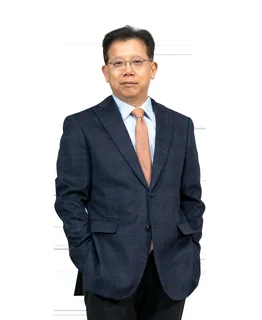
전석우 교수 사진

고려대학교신소재공학부

나노광전소재 연구실

전석우 교수, 특훈교수 (Seokwoo Jeon)

연구실 소개

이 연구실은 소프트 리소그라피와 proximity-field nanopatterning을 활용한 3차원 나노패터닝과 3차원 메타물질을 연구하며, 나노구조의 설계·제작과 광학·전기·기계·열 특성을 다룹니다. 또한 그래핀 양자점과 비산화 그래핀 플레이크 등 저차원 탄소 나노소재와 반도체 소자를 연구합니다.

AI가 연구실 홈페이지를 바탕으로 생성한 연구실 소개예요

연구실 홈페이지의 소개

Conventionally proposed 3D nanopatterning techniques have the capability to create various functions of 3D nanostructured materials that nature never provides. If it is possible to control and develop uniformly ordered 3D nano-architectures, we can build up new material properties. (e.g. photonic bandgap, negative refractive-index, and effective transport of energy and fluidics.) Furthermore, we can enhance mechanical, thermal, electrical, and optical properties of materials beyond intrinsic properties of bulk material. Our proximity-field nanopatterning (PnP) is a promising 3D nanofabrication technique with a specific structure design based on optics, simple materialization process, large pattern area, and high reproducibility. This technique can be applicable to many fields, including stretchable electronics, sensors, microfluidic devices, energy devices (thermoelectric and battery), and many others. 1. Low-dimensional carbon nanomaterials: Since the discovery of electrically conducting polymers (a discovery that led to the 2000 Nobel prize in chemistry), conjugated carbon based materials has been investigated for semiconducting, conducting, insulating and even light emitting layers of electronic and optoelectronic devices. The finding of fullerene in 1980s and carbon nanotube in early 1990s exploded the research field and recently found graphene filled the vacancy of 2D nanoelectronic material. The light-weight, flexibility, and supreme electronic and mechanical properties promise the usefulness of these materials to flexible electronics and mechanical and biological systems. 2. Three-dimensional nanostructured materials: The advent of nanoscience and technology is greatly indebted to the established techniques of micro/nanopatterning in past decades. Still, most of

원문 보기
연구 분야

소프트 리소그라피 · 3차원 나노패터닝 · 3차원 메타물질 · 그래핀 양자점 · 비산화 그래핀 플레이크

졸업생 진로

기업 10명

삼성전자 3 · SK하이닉스 2 · Contemporary Amperex Technology 1 · LG디스플레이 1 · Rio Tinto 1 · 삼성SDI 1 · Semiconductor Manufacturing International Corporation 1

학계 13명

가천대학교 1 · 고려대학교 1 · 공주대학교 1 · 단국대학교 1 · 신라대학교 1 · 한밭대학교 1 · 금오공과대학교 1 · 이화여자대학교 1 외 5곳

연구기관 5명

한국전기연구원 2 · 한국화학연구원 1 · 한국세라믹기술원 1 · US Naval Research Laboratory 1

연구실 홈페이지에 진로가 적힌 졸업생 28명을 AI가 집계했어요. 적히지 않은 졸업생은 빠져 있고, 지금 소속과 다를 수 있어요. 원문 보기

정보가 틀렸거나 삭제를 원하시면 [email protected]로 알려 주세요.

비슷한 연구를 하는 연구실