홈페이지의 모집 안내
“In addition to graduate students, we are actively recruiting motivated postdoctoral researchers in integrated photonic computing.”
원문에서 확인하기정보가 틀렸거나 삭제를 원하시면 [email protected]로 알려 주세요.
홈페이지의 모집 안내
“In addition to graduate students, we are actively recruiting motivated postdoctoral researchers in integrated photonic computing.”
원문에서 확인하기이 연구실은 정보 처리·통신·센싱을 위한 마이크로·나노스케일 포토닉스와 광전자공학을 연구합니다. 특히 포토닉 집적회로와 이종 집적을 중심으로 광전자 소자와 회로를 다룹니다.
AI가 연구실 홈페이지를 바탕으로 생성한 연구실 소개예요
연구실 홈페이지의 소개
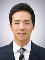
Our research group relies on the following technology platforms to facilitate information flows. (Click the triangle for more details.) Below is a glimpse of our recent research projects. Since 2010, our work has been supported by National Research Foundation of Korea, Institute of Information & communications Technology Planning & Evaluation, Agency for Defense Development, and Samsung Incubation Center for Future Technology. Our research group, led by Prof. Kyoungsik Yu at KAIST EE, is working on micro/nano-scale photonics and optoelectronics for advanced information processing, communications, and sensing. All the way from high-speed data center networks down to subwavelength-scale nanophotonic devices, we cover a broad range of optoelectronic devices and circuits with a special emphasis on photonic integrated circuits and their heterogeneous integration.
정보가 틀렸거나 삭제를 원하시면 [email protected]로 알려 주세요.
| 연구실 | 대학 | 주요 주제 | 구성원 | 비교 |
|---|---|---|---|---|
MetaPhotonics Research Lab함자 쿠르트 교수 | KAIST | 광학·포토닉스회로·칩 설계태양전지 | – | |
광자 시스템 연구실박남규 교수 | 서울대 | 광학·포토닉스회로·칩 설계 | 6 | |
Kim's Research group at KU김수진 교수모집 안내 | 고려대 | 광학·포토닉스반도체 소자나노소재 | 9 | |
나노 전자 및 신경망 모사 소자 연구실조병진 교수 | KAIST | 반도체 소자회로·칩 설계광학·포토닉스 | – | |
3D Integrated Opto-Electronic Device Laboratory김상현 교수 | KAIST | 반도체 소자회로·칩 설계광학·포토닉스 | 9 | |
나노전자시스템연구실이병훈 교수 | POSTECH | 광학·포토닉스센서·MEMS | – |